- 您现在的位置:买卖IC网 > Sheet目录3841 > PIC16C63A-04I/SO (Microchip Technology)IC MCU OTP 4KX14 PWM 28SOIC
2000 Microchip Technology Inc.
DS30605C-page 33
PIC16C63A/65B/73B/74B
5.3
PORTC and TRISC Registers
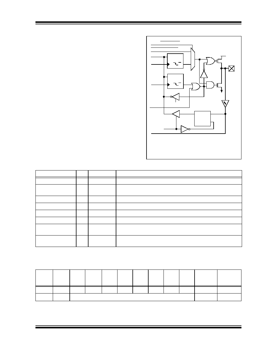
PORTC is an 8-bit bi-directional port. Each pin is indi-
vidually configurable as an input or output through the
TRISC register. PORTC is multiplexed with several
peripheral functions (Table 5-5). PORTC pins have
Schmitt Trigger input buffers.
When enabling peripheral functions, care should be
taken in defining TRIS bits for each PORTC pin. Some
peripherals override the TRIS bit to make a pin an out-
put, while other peripherals override the TRIS bit to
make a pin an input. Since the TRIS bit override is in
effect while the peripheral is enabled, read-modify-write
instructions (BSF, BCF, XORWF) with TRISC as des-
tination should be avoided. The user should refer to the
corresponding peripheral section for the correct TRIS
bit settings.
FIGURE 5-5:
PORTC BLOCK DIAGRAM
TABLE 5-5:
PORTC FUNCTIONS
TABLE 5-6:
SUMMARY OF REGISTERS ASSOCIATED WITH PORTC
PORT/PERIPHERAL Select(2)
Data Bus
WR
Port
WR
TRIS
RD
Data Latch
TRIS Latch
RD TRIS
Schmitt
Trigger
Q
D
Q
CK
QD
EN
Peripheral Data Out
0
1
Q
D
Q
CK
P
N
VDD
VSS
Port
Peripheral
OE(3)
Peripheral Input
I/O pin(1)
Note
1:
I/O pins have diode protection to VDD and VSS.
2:
Port/Peripheral select signal selects between port
data and peripheral output.
3:
Peripheral OE (output enable) is only activated if
peripheral select is active.
Name
Bit#
Buffer Type
Function
RC0/T1OSO/T1CKI
bit0
ST
Input/output port pin or Timer1 oscillator output/Timer1 clock input.
RC1/T1OSI/CCP2
bit1
ST
Input/output port pin or Timer1 oscillator input or Capture2 input/Compare2
output/PWM2 output.
RC2/CCP1
bit2
ST
Input/output port pin or Capture1 input/Compare1 output/PWM1 output.
RC3/SCK/SCL
bit3
ST
RC3 can also be the Synchronous Serial Clock for both SPI and I2C modes.
RC4/SDI/SDA
bit4
ST
RC4 can also be the SPI Data In (SPI mode) or Data I/O (I2C mode).
RC5/SDO
bit5
ST
Input/output port pin or Synchronous Serial Port Data output.
RC6/TX/CK
bit6
ST
Input/output port pin or USART Asynchronous Transmit, or USART
Synchronous Clock.
RC7/RX/DT
bit7
ST
Input/output port pin or USART Asynchronous Receive, or USART
Synchronous Data.
Legend: ST = Schmitt Trigger input
Address
Name
Bit 7
Bit 6
Bit 5
Bit 4
Bit 3
Bit 2
Bit 1
Bit 0
Value on:
POR,
BOR
Value on
all other
RESETS
07h
PORTC
RC7
RC6
RC5
RC4
RC3
RC2
RC1
RC0
xxxx xxxx
uuuu uuuu
87h
TRISC
PORTC Data Direction register
1111 1111
Legend: x = unknown, u = unchanged
发布紧急采购,3分钟左右您将得到回复。
相关PDF资料
52559-2270
CONN FFC 22POS .5MM VERT ZIF SMD
52559-1870
CONN FFC 18POS .5MM VERT ZIF SMD
DSPIC33EP64MC506-I/PT
IC DSC 16BIT 64KB FLASH 64TQFP
52745-1896
CONN FFC 18POS .5MM R/A ZIF SMD
PIC16LC622-04/P
IC MCU OTP 2KX14 COMP 18DIP
PIC16LF84A-04/P
IC MCU FLASH 1KX14 EE 18DIP
DSPIC30F1010-30I/MM
IC DSPIC MCU/DSP 6K 28QFN
52745-1696
CONN FFC 16POS .5MM R/A ZIF SMD
相关代理商/技术参数
PIC16C63A-04I/SP
功能描述:8位微控制器 -MCU 7KB 192 RAM 22 I/O RoHS:否 制造商:Silicon Labs 核心:8051 处理器系列:C8051F39x 数据总线宽度:8 bit 最大时钟频率:50 MHz 程序存储器大小:16 KB 数据 RAM 大小:1 KB 片上 ADC:Yes 工作电源电压:1.8 V to 3.6 V 工作温度范围:- 40 C to + 105 C 封装 / 箱体:QFN-20 安装风格:SMD/SMT
PIC16C63A-04I/SS
功能描述:8位微控制器 -MCU 7KB 192 RAM 22 I/O RoHS:否 制造商:Silicon Labs 核心:8051 处理器系列:C8051F39x 数据总线宽度:8 bit 最大时钟频率:50 MHz 程序存储器大小:16 KB 数据 RAM 大小:1 KB 片上 ADC:Yes 工作电源电压:1.8 V to 3.6 V 工作温度范围:- 40 C to + 105 C 封装 / 箱体:QFN-20 安装风格:SMD/SMT
PIC16C63A04SP
制造商:MICROCHIP 功能描述:NEW
PIC16C63A-20/SO
功能描述:8位微控制器 -MCU 7KB 192 RAM 22 I/O RoHS:否 制造商:Silicon Labs 核心:8051 处理器系列:C8051F39x 数据总线宽度:8 bit 最大时钟频率:50 MHz 程序存储器大小:16 KB 数据 RAM 大小:1 KB 片上 ADC:Yes 工作电源电压:1.8 V to 3.6 V 工作温度范围:- 40 C to + 105 C 封装 / 箱体:QFN-20 安装风格:SMD/SMT
PIC16C63A-20/SP
功能描述:8位微控制器 -MCU 7KB 192 RAM 22 I/O RoHS:否 制造商:Silicon Labs 核心:8051 处理器系列:C8051F39x 数据总线宽度:8 bit 最大时钟频率:50 MHz 程序存储器大小:16 KB 数据 RAM 大小:1 KB 片上 ADC:Yes 工作电源电压:1.8 V to 3.6 V 工作温度范围:- 40 C to + 105 C 封装 / 箱体:QFN-20 安装风格:SMD/SMT
PIC16C63A-20/SP
制造商:Microchip Technology Inc 功能描述:8 Bit Microcontroller Clock Speed:20MHz
PIC16C63A-20/SS
功能描述:8位微控制器 -MCU 7KB 192 RAM 22 I/O RoHS:否 制造商:Silicon Labs 核心:8051 处理器系列:C8051F39x 数据总线宽度:8 bit 最大时钟频率:50 MHz 程序存储器大小:16 KB 数据 RAM 大小:1 KB 片上 ADC:Yes 工作电源电压:1.8 V to 3.6 V 工作温度范围:- 40 C to + 105 C 封装 / 箱体:QFN-20 安装风格:SMD/SMT
PIC16C63A-20E/SO
功能描述:8位微控制器 -MCU 7KB 192 RAM 22 I/O RoHS:否 制造商:Silicon Labs 核心:8051 处理器系列:C8051F39x 数据总线宽度:8 bit 最大时钟频率:50 MHz 程序存储器大小:16 KB 数据 RAM 大小:1 KB 片上 ADC:Yes 工作电源电压:1.8 V to 3.6 V 工作温度范围:- 40 C to + 105 C 封装 / 箱体:QFN-20 安装风格:SMD/SMT